Tech Capability & Lab Infrastructure
APEON integrates precision molecular design and advanced material analysis for semiconductor, display, and 5G polymers. Our R&D team leads the entire process from initial design to pilot validation.
R&D Spotlight: Next-Generation Latent InitiatorsPatent Applications in Preparation
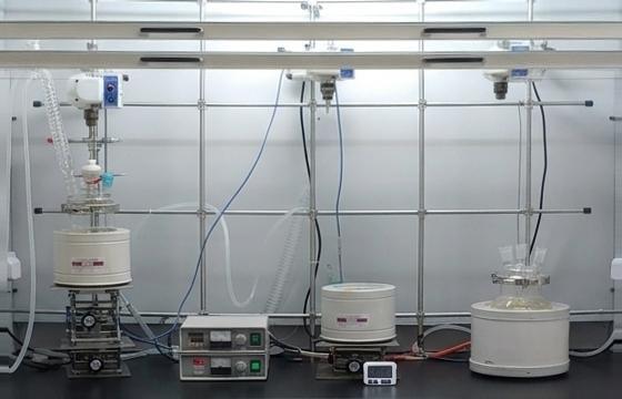
"In line with the advancing electronic materials industry, APEON's Advanced Materials Research Institute is actively developing next-generation latent initiators."
The electronics industry demands low-temperature processing and eco-compliance. Lower curing temperatures minimize CTE mismatch-induced warpage and stress, which is crucial for ultra-thin packaging. Meanwhile, strict regulations on hazardous substances like PFAS mandate a shift toward eco-friendly materials. Systems satisfying both requirements have become essential for next-generation supply chains.
APEON's Advanced Materials Research Institute is focusing on the R&D of next-generation latent initiators. Beyond basic DSC thermal analysis and viscosity evaluation, we have built a multi-dimensional cure-monitoring framework spanning dynamic mechanical analysis (DMA), thermomechanical analysis (TMA), and rheological behavior tracking, and by preemptively conducting long-term reliability evaluations under harsh conditions such as moisture penetration and severe thermal shock, we are elevating the maturity of our research toward commercialization.
Technical Background — The Latency Trade-off in Thermosetting Materials
Thermoset formulation faces a classic dilemma: low-temperature curability often means premature reaction during storage, shortening shelf life, whereas higher storage stability requires higher cure temperatures. To manage this trade-off, the industry extensively studies curing systems based on 'latency'—suppressing the reaction until a target temperature is reached. Reconciling latency with low-temperature reactivity remains a core research theme.
Regulatory Landscape — The Shift to Environmentally Compliant Curing Materials
Global chemical regulations like EU REACH are expanding scrutiny of PFAS, while antimony (Sb) compounds in some commercial curing systems face mounting substitution pressure due to toxicity concerns. The electronic materials industry now treats the transition to curing materials that reduce hazardous substance reliance—without sacrificing performance—as a shared challenge, driving active R&D worldwide.
* The institute is actively advancing this program, with the related patent applications in preparation. Detailed specifications (composition, properties, and performance data) will be disclosed in stages after filing; until then, product evaluation can proceed under NDA — please reach us via the Contact page.
1. Next-Generation R&D Initiatives
Display Materials R&D
Molecular design and polymerization research spanning commercial display ACF, commercialized low-Dk PI for 5G, and roadmap initiatives for 6G/mmWave low-loss materials.
A. [Pre-R&D] Self-Assembling ACF Binder
Advancing nano-phase separated binder and interfacial engineering research so conductive particles self-align to micro-electrodes in ultra-fine-pitch display bonding — targeting short-circuit suppression between fine terminals and improved fine-pitch electrical interconnection reliability.
B. 5G High-Frequency Low-Dk/Df MPI Adhesives
Proprietary modified PI (MPI) adhesives with reduced polar group density and fluorinated substituents to achieve low dielectric constant (Dk) and low dissipation factor (Df) in the 28 GHz band — a qualified supply history with mobile flagship devices established via grades such as APC-4310.
C. [Technology Roadmap] 6G/mmWave Ultra-Low-Loss MPI
Planning mid-to-long-term research on fluorinated low-polarity PI and ultra-low-loss MPI for mmWave and 6G bands. A Df ~0.002–0.003 target remains at the roadmap review stage.
Semiconductor & EV Materials R&D
High-temperature polymer engineering for QFN packaging NPI, high-density semiconductor stacking, and EV battery insulation and thermal management (heat dissipation via thermally conductive fillers).
A. QFN Semiconductor Packaging Hybrid Adhesive
Imide-urethane hybrid adhesive (APC-4320) for QFN backside protection and repeated 260°C lead-free reflow — post-cure Tg 105°C and high crosslink density designed to retain bond strength through multiple reflow cycles. NPI and line evaluation ongoing.
B. [Technology Roadmap] HBM Hybrid Stacking Materials
Planning mid-to-long-term research on solvent-free imide-epoxy hybrid resins for HBM and chiplet stacking. Exploratory PSPI dielectric layer synthesis and custom formulation in parallel.
C. [Pre-R&D] EV Battery & Power Module Resin
Developing urethane/imide hybrid resins that provide electrical insulation and metal-frame adhesion, with thermal management (heat dissipation) enabled through thermally conductive fillers, aiming to mitigate thermal runaway propagation during fast charging.
2. Core Polymer Synthesis Platforms
Polyimide & TPI Synthesis
Thermoplastic polyimide (TPI) varnish synthesis utilizing steric hindrance and flexible monomer copolymerization to achieve solution processability and sub-300°C melt flowability. By targeting moderate Tg, we enable 150–200°C fusion-bonding while maintaining excellent thermal stability (Td > 400°C).
Polyurethane Precision Synthesis
Core technology for synthesizing high-performance polyurethanes through precise reaction design of polyols and isocyanates.
Imide-Urethane Segmented Copolymers
Segmented copolymerization linking rigid imide rings with flexible urethane segments in a single backbone. Polyurethane-imide-acrylate (PUIA) adhesives designed for 260°C lead-free reflow stress resistance.
Battery Binder Technology (Pre-R&D)
Exploratory research on high-elasticity binders to suppress volume expansion and prevent cracking in next-generation silicon anodes. We incorporate rigid imide segments into a waterborne polyurethane matrix, designing for sub-200°C processing to ensure copper current-collector compatibility.
Functional Groups & LFB Control
Introduction of reactive functional groups (epoxy, carboxyl, acrylate) at the polymer terminals and pendant positions. End-capping agents for network density control, low-temperature fast bonding (LFB), and residue-free peel release development.
Scale-up & Process Engineering
Process scale-up engineering from lab-scale (1L) to pilot-scale (50L) and commercial mass production. Lot-to-lot consistency and reproducibility based on reaction kinetics and heat-transfer data.
3. Instrumentation & Lab Capabilities
Chemical Structure & Chromatography
- GPC/SEC (Gel Permeation Chromatography)Measures molecular weight distribution (Mn, Mw, dispersity Đ / PDI) to control resin consistency.
- FT-IR (Infrared Spectrometer)Monitors the degree of imidization (DOI) and quantifies residual acrylate functional groups after cure.
- Karl Fischer Titrator (Trace Moisture Analysis)Detects trace moisture levels (ppm) that cause void defects during lamination.
Thermal & Rheological Analysis
- DMA (Dynamic Mechanical Analyzer)Measures tensile storage and loss moduli (E′/E″) versus temperature for film viscoelastic and thermal stress-relaxation analysis.
- DSC (Differential Scanning Calorimeter)Measures glass transition temperature (Tg) and profiles cure kinetics.
- TGA (Thermogravimetric Analyzer)Determines 5% weight loss temperature (Td5) under a nitrogen atmosphere.
- Rheometer (Rotational / Oscillatory)Measures shear storage/loss moduli (G′/G″) and complex viscosity for ACF thermocompression flow and cure-behavior analysis.
Adhesion & Reliability Testing
- UTM (Universal Testing Machine)Measures 90°/180° peel strength, tensile properties, and die shear parameters.
- Temperature & Humidity ChamberExposes specimens to 85°C/85% RH for up to 1,000 hours to evaluate moisture resistance.
- Reflow SimulatorSimulates repeated 260°C lead-free solder reflow to check for delamination and the suppression of outgassing-induced micro-voids.
4. Commercial Success & Supply-Chain Localization
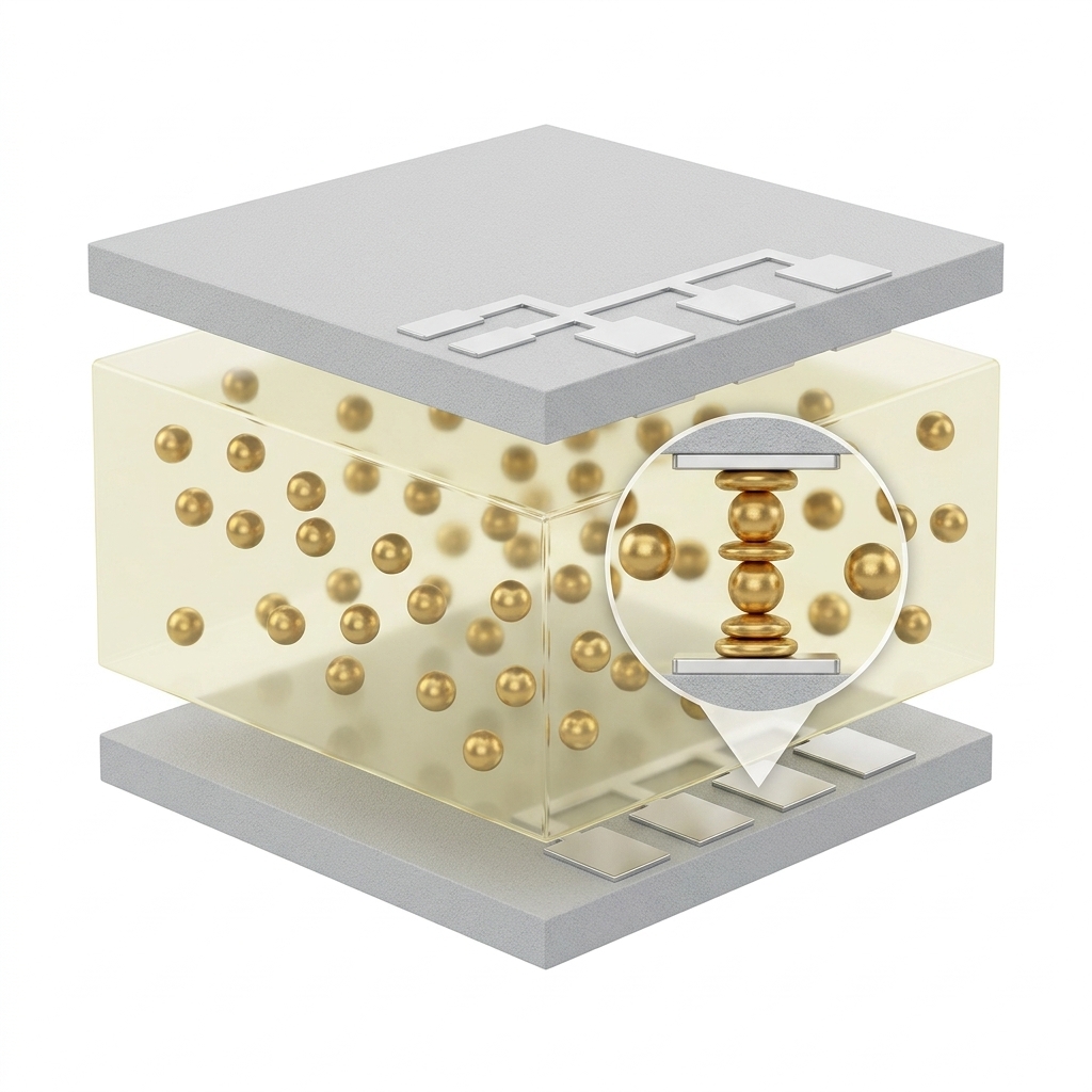
Display Anisotropic Conductive Film (ACF) Binder
Developed polyurethane-imide binders for fine-pitch driver IC packaging (ACF). Line evaluation and NPI supply ongoing with global display customers.
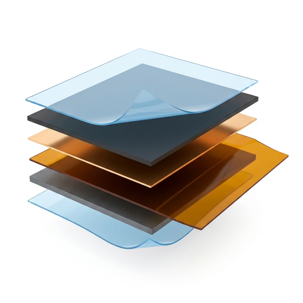
FPCB High-Temperature Adhesives & EMI Shielding Film Resins (Localized Supply)
Successfully localized high-temperature FPCB adhesive resins — previously import-dependent — via our in-house synthesis route. Supplied to major circuit-board manufacturers, contributing to the self-sufficiency of Korea's IT supply chain.
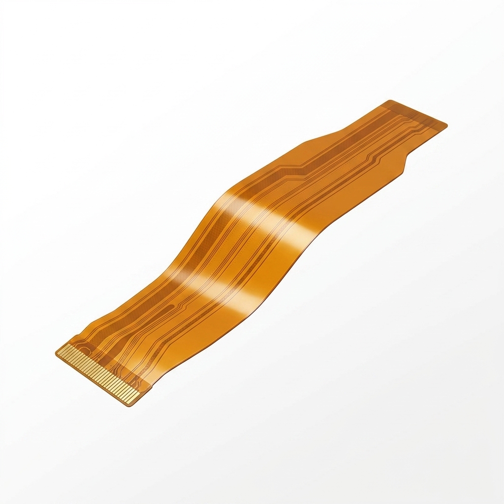
5G High-Frequency Low-Loss (Low Dk/Df) Adhesives
Engineered modified polyimides incorporating bulky, low-polarity units. Successfully achieved low dielectric constant (Dk) and dissipation factor (Df) at 28 GHz, establishing a qualified supply history with mobile flagship devices.
5. Intellectual Property & Patents
Patent: (Meth)acrylate-terminated polyurethane (amide) imide adhesive resin, manufacturing method and use thereof
Application covering the composition, synthesis, and uses of (meth)acrylate-terminated polyurethane(amide)imide adhesives with covalently linked imide and urethane units.
Patent: Low dielectric polyamideimide-based adhesive resin, manufacturing method and use thereof
Application for low-dielectric PAI adhesive compositions and their preparation and uses, using structural design to reduce molecular packing and lower Dk/Df.
Patent: Polyamideimide resin for semiconductor package, manufacturing method and QFN adhesive film
Application for PAI resins with silicone segments for semiconductor packages and QFN adhesive films made therefrom — covering composition, synthesis, and uses.